Categories
Test Gear

Eurorack module prototyping and testing power supply thing: Part 3

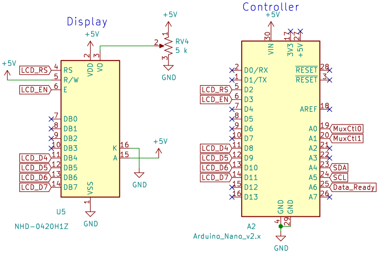
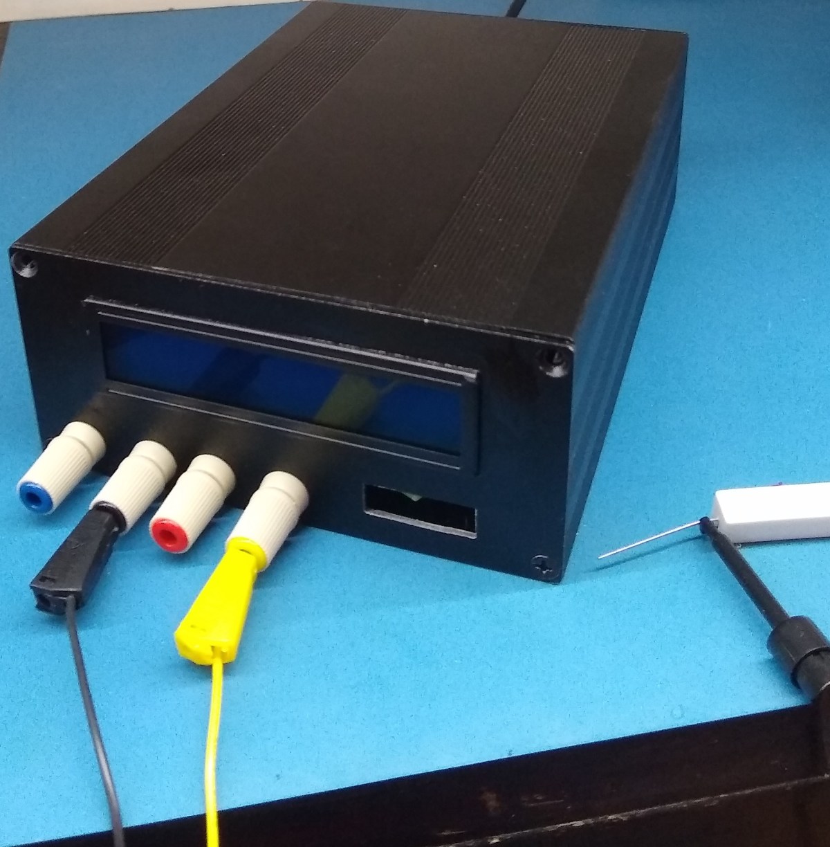
In part 1 we decided I need a power supply and picked out a few basic components. In part 2 we looked at display and control.  And now we’re going to start looking at current measurement.

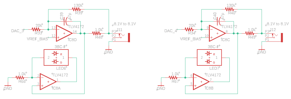
For the purposes of discussion I’m going to divide current measurement up into three parts: Analog to Digital Converter, Sensor, Amplifier. This is the approximate order I picked out components and design patterns; however there was a fair amount of iteration in each area before reaching the final configuration. The sections function pretty much as described. The analog to digital converter makes the analog measurement useable by the digital micro controller. The sensor converts the parameter we’re trying to measure into a voltage. And the amplifier matches the output range of the sensor to the input range of the converter. Since the amplifier is the most detailed it’s getting its own post.

Analog to Digital Converter

I’ve wanted to try a high bit external analog to digital converter (A/D) for a while and this seemed like a good opportunity. Additionally, while the Arduino does have an onboard A/D, it’s only 10 bits. Based on the target measurement range (1-400 mA) a 10 bit A/D means there’s two bits per mA making conversion the limiting factor in measurement resolution which is usually something you’d try to avoid. After looking at a couple of different options I picked out a NAU7802 24 bit A/D for three reasons: 24 bit is plenty of resolution for this project, it communicates via I2C which should be relatively easy to communicate with the Arduino, and it is very cost competitive.

Step one with the A/D is to have it talk to the microcontroller and take some readings to see how well behaved it is. I wired up the converter using the recommended circuit from the datasheet except I replaced the Wien bridge with my Heathkit variable output power supply to provide a range of voltages to the measurement pins. I quickly discovered that Vin1N pin needed to be connected to Vref/2 since the output was a signed 24 bit number, and to get negative numbers the voltage on Vin1P needed to be less than the voltage on Vin1N. I also noticed some other anomalies near the extremes of the input voltage range.

I didn’t dig too far into the source of these anomalies. They represent a range reduction of <10% and I was only planning on using 80% of the range anyway; so, I designed around the anomalies. This was accomplished in two parts first I would have the amplification stage linearly bias the measurement by ~100 mV so that operation was always in a region above the lower anomaly and then I’d set the sensor amplification so that 400 mA resulted in an input to the A/D of ~2.5 V.

The Sensor

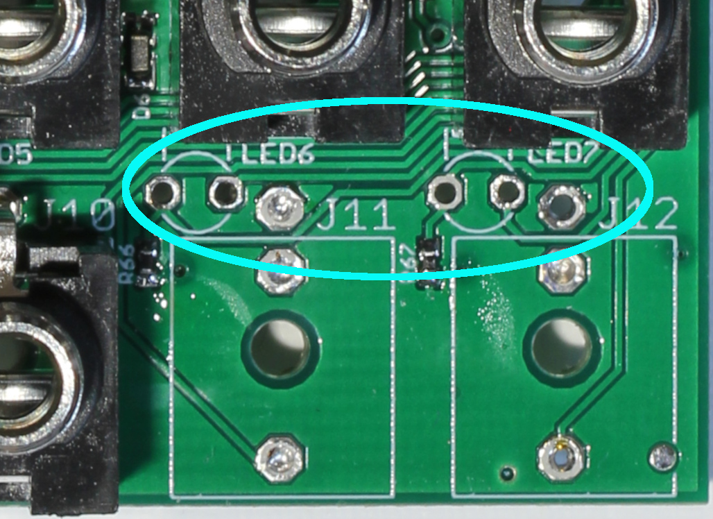
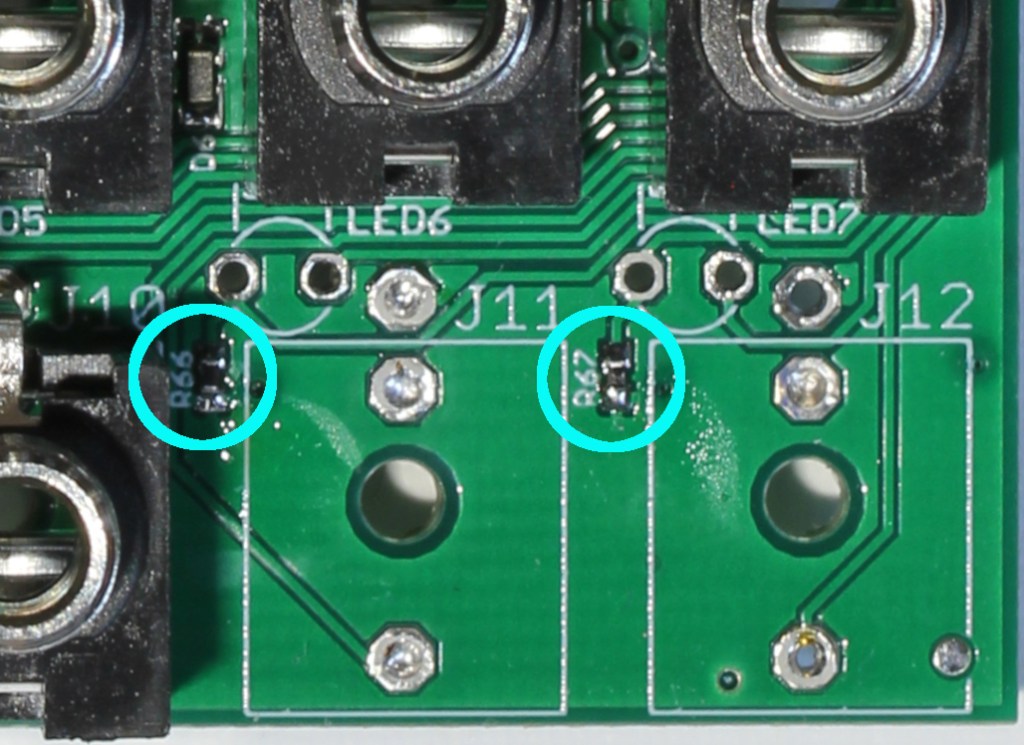
Three common sensors for current measurement are a current sense transformer, a Hall effect sensor, and a current sense resistor. The goal hear is to measure the mA being consumed by the load attached to each output channel. It’s expected that the loads will be primarily DC so the current sense transformer won’t be useful. Since three sensors are required price is a concern and hall effect sensors tend to run few dollars each where as current sense resistors are $0.25-$0.50. So what is a current sense resistor? Well it’s a resistor it converts current to voltage using Ohm’s law. While any resistor can be used for current measurement typically to be classified as current sense a resistor three factors will be considered. low resistance (< 100 mΩ) so that minimal voltage drop out occurs between the source and the load, tight tolerance (< ±1%) so that measurements are consistent across circuits and relatively high power (> 0.5 W). Additionally if you’re measuring a wide current range you may look for one made using a low thermal coefficient of resistance material. A wide range of measured currents means the resistor will operate over a wider range of temperatures, and having a stable resistance over a range of temperatures means readings will be more stable. For this project I picked a 50 mΩ ±0.5% 0805 chip resistor.

Categories
Test Gear

Eurorack module prototyping and testing power supply thing: Part 2

Previously we decided I needed a better lab power supply for working synth modules; picked out a switch mode power supply to do most of the heavy lifting,, a case, and desirable output terminals. This time we’re going to look at the electrical design that will generate the three output voltages ±12 V and 5 V, and how current will be measured and displayed.

The Display

Let’s start with the easy stuff. I want the display to do two things let me know the system is on and display the output currents for each output voltage. To accomplish goal one I’ll pick an LCD with a back light which is nearly all of them.

Goal two is slightly more challenging. We need to pick the number of digits displayed and the display format. That is will all channels be displayed at the same time or will they be displayed one at a time? If they’re displayed one at a time how will we transition between which measurement is displayed. The number of digits displayed should be based on the current consumption for euro rack modules. From what I’ve seen this ranges from ~10 mA to ~200 mA. So we’ll want three characters for the measurement, two characters for units and an additional character to separate the measurements. For the overall format I wanted to see all of the measurements at the same time (Two other display options cycling between measurements using a switch or a timer seem fiddly). So with three channels and six characters per channel I need a display that’s at least 18 characters long; fortunately I have a 2×24 character display.

The final thing required for the display is a micro controller to take the output of the current sensor and write it to the display. I didn’t want to break any new ground here and just grabbed the nearest Arduino nano.

Circuit wise the display and controller look like this. the display has a typical 16 pin interface, and I’m using the four bit data transfer protocol.

Output voltage generation

For regulation I picked out a couple of classic regulators the LM317 and LM337. These are adjustable regulators so I picked out some 5 k multi turn pots to trim the output to the desired voltages. Finally, I followed the reference design in the datasheet for sizing and laying out the capacitors and diodes. For the 5 V output initially I duplicated the circuit configuration for the 12 V rail to minimize the part count on the BOM, and got all the way to ordering boards before realizing this would be a bad idea. Why is it terrible? glad you asked. On initial assembly the prior to tuning the output with the trim pot the regulator output could be anywhere between 0-14 V. The display and controller are powered from the 5 V rail and do not react well to voltages over about 6 V. Thus in the original configuration shown below a good portion of the project could be smoked just by turning it on for the first time. So I changed the 317 for the 5 V rail to a fixed output 5 V regulator for the first revision.

Next time in this series we’ll take a look at current measurement.

Categories
Test Gear

Eurorack module prototyping and testing power supply thing: Part 1

I was looking at my workbench not too long ago

Ahhh

And I thought if I had a ‘real’ power supply with banana jack connectors most of this rat’s nest would get cleaned up. In addition to the mess, the ATX supply + converter board has some other problems. Most notably that the 24 pin cable is fairly stiff which pushes the converter board into the work area and since the ground and power terminals are close to each other this makes it easy to short and I have blown a couple of fuses on it. Now if I was sane I would pick up a used HP3630. It’s a pretty typical triple output power supply perfect for prototyping a euro rack module. However I’m just a little crazy so I’ve decided to build my own.

Let’s see how far I get before I decide to go buy an HP3630.

Specifications

The basic design is to output three voltages: +12 V, -12 V, and +5 V. Output connections will be made via banana jacks and a 16 pin IDC connector the same the would be used to power a euro rack module in the rack. The point of this project is to reduce the three intermediate steps I use now to a single step. So the power supply should plug directly into the wall with all of the associated fun stuff that implies.

Everything above can be handled with a ±12 V output switching supply and a regulator to get 5 V. So I decided to add current measurement and display for each of the output voltages.

Design – Switching supply

To start designing a switching supply is going to be way to complicated for this project so I decided to purchase one. Based on my previous experience with Meanwell supplies I picked a ±15 V dual output supply. Using 15 V instead of 12 V means that any opamps used as part of the the current measurement won’t have to run on the high rail; as well as, allowing any output irregularities to be trimmed out with regulators.

The Case

Now that the switching supply has been chosen and get a rough idea of how big of a case to use for the project. I picked a ~20x15x7 cm case and stared drilling.

Next time we’ll take a look at regulation and the display.

Categories
Eurorack Module Design

Chord Arpeggiator Design: Part 3

Previously in part 1 we diagramed a state machine to represent a chord arpeggio. In part 2 we determined what the sum of products would be for the state transition logic, and simulated the logic. Now it’s time for the next step which is to look at the physical implementation. I spent some time KiCAD and came up with this lovely schematic.

Ok so that’s 10 logic chips. We haven’t even looked at input conditioning, any manipulation of the clock that may need to be done, and actually generating an output control voltage from the various states. This is the point where I decide the module would be better implemented with a microcontroller, the scope expands out of control (because microcontrollers can do anything, why stop with 4-6 note sequences, why limit things to major and minor chords? What if I want to arpeggiate over a Cdim add 9 because I’m insane), and ultimately shelve the idea until a future date.

Categories
Eurorack Module Design

Chord Arpeggiator Design: Part 2

Last time I started designing a chord arpeggiator. We got as far as and articulating the specifications and then drawing a state machine to handle note transitions. Today we’ll try to minimize the gate count for transitioning between states and then simulate the logic using VHDL.

Logic Minimization

I decided to use Karnaugh Maps because I actually remember how to use them, and with only 8 variables the problem is still simple enough so that real logic minimization tools aren’t necessary yet. But ‘Aha!’ you say you have 10 variables 6 states and 4 inputs. Well since only one state can be active at a time the corresponding up and down states can be combined when working out the logic. To reduce typing I After working through the Karnaugh Map for each state I got this

  • States
    • Fundamental
    • Third
    • Fifth
    • Seventh
    • Fifth_down
    • Third_down
  • Inputs
    • Third_on
    • Fifth_on
    • Seventh_on
    • Decending_on
  • Logic
    • Fundamental = (not Third_on and not Fifth_on and not Seventh_on ) or (Third and not Fifth_on and not Seventh_on ) or ( Fifth and not Seventh_on and not Decending_on ) or ( Seventh and not Decending_on ) or ( Seventh and Decending_on and not Third_on and not Fifth_on ) or ( Fifth_down and not Third_on and Decending_on ) or ( Third_down and Decending_on )
    • Third = ( Fundamental and Third_on )
    • Fifth = ( Fundamental and not Third_on and Fifth_on ) or ( Third and Fifth_on )
    • Seventh = ( Fifth and Seventh_on ) or ( Third and not Fifth_on and Seventh_on ) or ( Fundamental and not Third_on and not Fifth_on and Seventh_on )
    • Fifth_down = ( Seventh and Fifth_on and Decending_on )
    • Third_down = ( Seventh and Third_on and not Fifth_on and Decending_on ) or ( Fifth_down and Third_on and Decending_on)

if I was actually good at digital design I’d be able to simplify that down to something ridiculous like 3 NAND and 2 XOR gates. But I’m not and that is a lot of logic which means there’s probably some errors in it and we should do a simulation.

Simulation

For simulating this type of glue logic I like to write a program for an FPGA and see how it runs. Of course I don’t have an actual FPGA or FPGA programming tool since they’re pretty spendy. So, I use the next best thing a web base FPGA simulator called EDA Playground because it’s free and easy to use. There are a variety of FPGA programming languages to choose from on EDA Playground. I picked VHDL because I remember how to use it the best of the available languages.

Link to EDA Playground arpeggiator simulation. While not my finest code it does show that the logic works. And EDA Playground provides a nice timing diagram for visualization.

VHDL simulation output

Now that the logic is validated join me next time when we look at what the physical implementation of this thing will look like.

Categories
Eurorack Module Design

Chord Arpeggiator Design: Part 1

Today’s Post is brought to you by my latest questionable module idea that probably only I am interested in. The idea is a four note chord arpeggiator. And not just four notes that would be boring I want to be able to toggle whether a note is played, toggle if the arpeggio is ascending only or will ascend and descend, and toggle some of the notes so the module can switch between major and minor chords and Major and Major 7 chords. Yes, I know just enough Baroque music theory to be dangerous. Back to the task at hand. And as always let’s try to do this without a microcontroller.

Specs

  • Up to 4 notes will be played
    • Notes 2-4 will be toggleable
  • Fundamental will be from CV input
  • 2nd note is toggle able between major and minor 3rd
  • 3rd note is a 5th above fundamental
  • 4th note is toggleable between 7th and full octave
  • Output will be in 1 V/Octave
  • Changes to next note on clock pulse input
  • No micro

Design

If the module was going to transition between notes in a predictable order all the time we could use a shift register to handle the transitions. Since the transitions proposed are a little more complicated I decided to use a finite state machine to help design handle the transitions between notes.

What is a finite state machine? It is an abstract model of a system that can be in exactly one of a fixed number of states at a time. Such as a combination lock or a traffic light. Since we’ll only want to output one note of the chord at a time, and the clock input can indicate transition between notes/states, the state machine seems like a reasonable way to approach the problem.

Next we’ll need to simplify thing a little bit Since it is unlikely that both the major and minor third would be played in the same sequence I went ahead and grouped those into the same state. Likewise the seventh and full octave states were grouped. I decided to give descending fifth and thirds their own states. The alternative would be to use a separate ‘current direction’ state, but this way seems lazier. We’ve got 6 states and I suspect it will be easy to find an 8 bit register/d-flop/latch block so no worries there. With the states defined all that remains is defining the transitions between the states. For that we’ll need to articulate the module inputs. I’ve come up with four inputs affecting the state machine

  • 3rd Active
  • 5th Active
  • 7th Active
  • Descending Active

If the 3rd and 7th inputs are active and the 5th and Descending inputs are inactive that’ll produce note patterns of 1-3-7-1-3-7. If Descending is enabled the pattern will change to 1-3-7-3-1-3-7. This is going to get old fast so I’m just going to draw a graphical representation.

The circles represent the states the arrows represent possible transitions. If I were more ambitious I’d include some indication of the logic for each transition.

Join me next time when I start turning the graphical state machine into implementable logic.

Categories
DIY Mutable Instruments

Tides 2 LEDs

I’ve put together a few Mutable Tides 2 modules, and I think just about all of them have LED problems. Today we’re going to be looking at LED6 and LED7 which are among the audio jacks on the lower right of the board. As always it’s a good idea to look at the schematic.

Not much going on here so it should be easy to troubleshoot. We’ve got a buffer amp driving the LED and a current limiting resistor. Circuits for LED6 and LED7 are duplicates which is nice since they’re probably suffering from the same problem. The first thing to do in these situations is to check the signal. I like to start with the op amp to make sure it’s outputting something. Next making sure Pin 1 on the LED matches the op amp output will give you an idea of trace integrity. Since the signal to pin one of the LEDs looked good I assumed the LEDs must be bad and removed them. And this was wrong. With the LEDs out it became apparent that the LED Pin 2 net was floating. And connecting the LEDs to my bench supply showed they worked fine. So the actual culprits here were the R66 and R67 resistors which had bad solder joints. Visual inspection showed that the resistors were slightly misplaced and only one solder joint had formed properly. After removing the J11 and J12 jacks this was easily fixed by adding a little more solder.

Tides 2 R66 and R67 on the PCB

If I could remember how soldering this board went a few months back I suspect these resistors tombstoned. Tombstoning is when one terminal of a two terminal part lifts into the air during solder reflow. In the classic example the part stands perpendicular to the face of the PCB and looks like a tombstone.

Tombstoned SMD resistors, Courtesy of O-fey and Wikimedia commons

Primarily tombstoning has to do with asymmetrical heating of the pads for small surface mount components. Since Tides 2 uses almost entirely 0402 sized passives and I reflow solder the boards on a hotplate with a noticeable temperature gradient between the center and the edge, I had quite a few tombstoned parts.

One of the things I like about reflowing on a hot plate is it’s easy to adjust parts while the solder is melted. So I can just tilt tombstoned parts back into position with some tweezers and forget about them. Unfortunately with parts this small it’s easy to knock the parts out of alignment and miss one of the solder pads. The lesson here is I should be better about using a microscope during reflow.

Categories
LRR Eurorack Modules

JVCA Eurorack Module

This Eurorack module contains 2 JFET based voltage-controlled amplifiers (VCA). VCA’s are a core component in synths. They’re commonly used in conjunction with an envelope generator for shaping
sounds, or with two oscillators for tone synthesis. The inputs and outputs are buffered using fast professional audio grade op-amps to maintain signal integrity and performance.

Specs

SizeWidth: 4 HP
Depth: 42 mm
Power360 mW
12 V15 mA
-12 V15 mA
Channel
Definitions
1 (knob)User control knob/
CV DC offset
2 (CV)Control Voltage
0 to 5 V range
3 (SIG:IN)Input Signal
-5 to +5 V range
4 (SIG:OUT)Output Signal

Power

The module uses a standard 10 pin Eurorack connector with polarity marked

Inputs and Outputs

1. Knob

Adds a DC offset from 0 to 5 volts to the control voltage.

2. CV

This is the control voltage gain input, and it is normalized to 0 V. The recommended input range is 0 to 5 V. Voltages less than 0 will have the same gain as 0 V, and Voltages greater than 5 V will have the same gain as 5 volts.

3. Sig:In

The signal input is DC-coupled and will accept audio or CV signals. The recommended input range is -5 to +5 V. Voltages outside this range will cause increased distortion.

4. Sig:Out

Signal output

Inputs are tolerant to voltages from -12 V to + 12 V. Exceeding this range will damage the module.

Gain Response

The response of the VCA is exponential. A representative plot showing gain vs control voltage is shown in Figure 1.

Figure 1. Gain vs Control Voltage

Categories
DIY Mutable Instruments

Ambiguous STM32 part marking

So you want to DIY a Mutable Instruments Module

A few months ago, I was assembling a Mutable Instruments module (let’s assume it was Rings), and I was about to place the microcontroller. We all know that Pin 1 IC packages are marked with some sort of dimple, dot, or indentation. For example

Pin 1 designator

However, this microcontroller had two two dimples.

So which one marks Pin 1? If you’re literate you read the datasheet, and note that Pin 1 is denoted by the dimple at the bottom left of the text marking.

Mechanical drawing by STM

If you’re illiterate, like me, you ignore the datasheet, decide that pin one must be the big dimple near the top of the text, install the part backwards, rage at the world when the module doesn’t work., heat gun the micro controller off, replace it with a new IC oriented correctly, and then wonder why you weren’t smart enough to read the documentation in the first place.

The moral of todays story is when in doubt read the documentation. In fact just read the documentation, always.

Categories
Eurorack Module Design

ADSR Design Part III

After seeing how the ARP2600 implemented an ADSR. I’ve decided to pencil in the Decay and Sustain parts to my AR design.

Decay

Starting with the Decay stage. This will be similar to the Release stage. So we’ll just copy and paste the input mix and exponential converter. from that stage. Things diverge a bit with the current sink for decay because the output capacitor will be discharged to the sustain voltage instead of ground. So the fancy bi directional current source from the Release is getting replaced with a classic voltage controlled current sink design.

Decay Current sink

With this design if the control voltage is below the sustain voltage the MOSFET controlling current flow will be off. We can take advantage of this by using an enable to short the control voltage input to ground which will result in the current sink being off. It also means that the sustain voltage needs to be mixed with the decay control voltage in order to reliably discharge the output capacitor during the decay phase. The final note is that the size of the current sense resistor, R20, is going to have to be picked carefully. While the output voltage is higher than the control voltage the voltage change will be linear. Once the output voltage drops below the control voltage the op-amp will turn the current limiting FET, Q4, fully on and the remainder of the decay transition will be a regular RC discharge curve to the sustain voltage as seen below.

If we want to keep the linear voltage transitions from the Attack and Release stages then the current sense resistor needs to have a low value. However a low value resistor means a smaller control voltage range which means the system will be more susceptible to noise. The best solution here is probably to just try a couple values for the current sense resistor during prototyping and see how they sound.

Sustain

Moving on to the sustain. The ARP2600 used a BJT, a capacitor and a potentiometer to set the sustain level. Since using CV is part of the design constraints it makes sense to use an op-amp to add the CV and control pot voltages. As the op-amp can perform the function of both the BJT and the capacitor in the original design we can drop those leaving us with.

Final Thoughts on the ADSR

This design uses fewer ICs than I was originally anticipating. I will probably try to prototype it at some point.