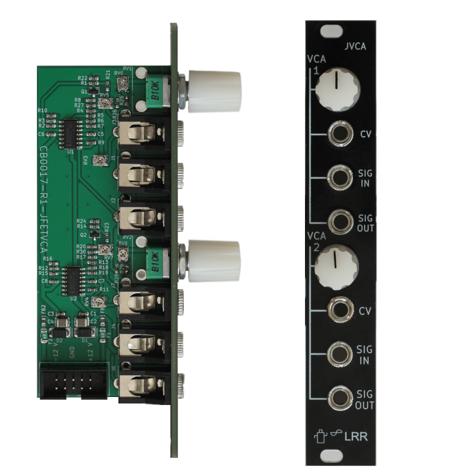
This Eurorack module contains 2 JFET based voltage-controlled amplifiers (VCA). VCA’s are a core component in synths. They’re commonly used in conjunction with an envelope generator for shaping sounds, or with two oscillators for tone synthesis. The inputs and outputs are buffered using fast professional audio grade op-amps to maintain signal integrity and performance.
Specs
Size
Width: 4 HP Depth: 42 mm
Power
360 mW
12 V
15 mA
-12 V
15 mA
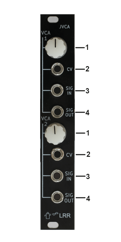
Channel Definitions
1 (knob)
User control knob/ CV DC offset
2 (CV)
Control Voltage 0 to 5 V range
3 (SIG:IN)
Input Signal -5 to +5 V range
4 (SIG:OUT)
Output Signal
Power
The module uses a standard 10 pin Eurorack connector with polarity marked
Inputs and Outputs
1. Knob
Adds a DC offset from 0 to 5 volts to the control voltage.
2. CV
This is the control voltage gain input, and it is normalized to 0 V. The recommended input range is 0 to 5 V. Voltages less than 0 will have the same gain as 0 V, and Voltages greater than 5 V will have the same gain as 5 volts.
3. Sig:In
The signal input is DC-coupled and will accept audio or CV signals. The recommended input range is -5 to +5 V. Voltages outside this range will cause increased distortion.
4. Sig:Out
Signal output
Inputs are tolerant to voltages from -12 V to + 12 V. Exceeding this range will damage the module.
Gain Response
The response of the VCA is exponential. A representative plot showing gain vs control voltage is shown in Figure 1.
Previously I blocked in and picked some basic circuit designs for the Attack part of the AR module, and we learned some things looking at how the ARP2600 handled envelope generation. This time we’re going to expand the ‘control logic block’ to control when the capacitor is charging and discharging. Also I’ve picked out a few component values and calculated the range of control voltages and the range of charging currents and it looks like modifications will be needed. And lastly there’ll be a bit about the release block.
Controls
Last time we decided to ditching trying to time things and just use input and feedback control to enable charging the output capacitor. First the conditions for enabling the attack current source need to be described. The attack current source should be enabled if the Gate input signal is high and the output of the module is below the output set point. In circuit form that’s going to look something like this.
A comparator compares the current output with the setpoint. If the setpoint is higher than the output the comparator outputs a logic high value. If the gate is also high the AND gate outputs high and the Attack current source is enabled. A feedback resistor may need to be added to the comparator to prevent rapid toggling thus making the comparator a Schmitt Trigger. I also would like to note that this control set up will ‘top up’ the output capacitor if the gate is especially long and the capacitor begins to self discharge.
Math
This brings us to the part of the design where we need to pick some component values and transition times and start doing math to see if other component values are reasonable. Here are the initial choices.
Output Capacitor (C)
10 µF
Charge time min (tmin)
1 ms
Charge time max (tmax)
10 s
Output Voltage minimum (Vmin)
0 V
Output Voltage maximum (Vmax)
5 V
Now using the terminal equation for a capacitor
I = C dV/dt
and the input voltage output current relationship for the current source
Iout = 1/R * (Vcc – Vin)
The minimum and maximum charging currents and control voltages can be calculated.
Charge Time
Iout
Vin
1 ms
50 mA
2 V
10 ms
5 mA
11.9 V
1 s
50 µA
11.99 V
10 s
5 µA
11.999 V
Current Range
The output current range seems ok. 5 µA is on the small side, but we’ll have to actually build a prototype to see if it’s too small to work.
Voltage Range
The range for Vin however is immediately problematic for two reasons that require circuit adjustments.
First in order to have a long attack time Vin needs to be approximately the same as Vcc (on the order of 1 mV), and having inputs and outputs of an op amp at either of the power rails tends to cause unpredictable behavior. The ‘rail to rail’ op amps I usually use recommend operating 25 mV to 1 V from the rail for ideal performance. Additionally output current is related to the difference between Vcc and Vin. Vin is controlled and Vcc is 12 V, or is it? Vcc could be higher or lower depending on the power supply and the power input protection. The typical power input block I use for circuit protection and power filtering can drop the input voltage 10’s of mV. So referencing the control current to Vcc is going to cause unpredictable behavior.
So I’m swapping the current source for this one, which uses sources a current proportional to Vin, and has the added benefit of acting as a current sink, so an identical set up can be used as part of the release stage. A limiting factor here will be the maximum current output of the op amps and 50 mA is getting up there.
The second issue is that charge time and by extension input voltage covers 4 orders of magnitude. The table shows that input voltage difference between 1 s attack time and 10 s attack time is 9 mV while . So as is more of the input space for the module is devoted to short attack (and by extension release) times. This use of the input space is backwards to human perception that is it’s easier for humans to notice the difference between 1 s and 10 s than it is for us to notice the difference between 1 ms and 10 ms. So we want to convert a linear voltage input into an exponential voltage input to better match the control voltage to attack time to human perception. Fortunately there’s a pretty typical circuit for that.
Release block
At this point the release block is super easy. It’ll be identical to the Attack block with the following changes. The input voltage to the current source needs to be negative to make it a current sink. The control logic needs to be inverted. That is on when the gate signal is low and the output voltage is above 0 V.
The next module I’m designing is an envelope generator. Since, I’m doing this while I wait for boards and part for other modules, I’ve decided to do a better job documenting the early part of the deign; so, if this project gets shelved for a bit I can spend less time remembering where the design is at. Now on to the fun bits.
What is an Envelope Generator
In signals an envelope describes how the signal changes in time. Since I’m primarily working with synths, the signal is going to be sound. To make a synth envelope an envelope generator outputs a sequence of voltages that are typically used as control voltages for an amplifier or filter. For example an envelope (blue) is used to control the amplitude of a sine wave (pink) using a voltage controlled amplifier.
Envelope example
A Block Diagram
How do we create a sequence of voltages? To start with lets put together a block diagram for a four part envelope generator commonly referred to as an ADSR (attack, decay, sustain, release).
ADSR block diagram
I’ve expanded the A block to show likely sub-blocks the DSR blocks will contain similar sub-blocks. Working our way through the blocks. The inputs to the A stage, CV and control knob voltages, will be combined (probably added). The mixed control voltages will be fed to the driver block, where the control voltages will be interpreted into a signal to send to the memory block. The mixed control voltages will also be fed into a timer. When triggered the timer will close the switch between the driver and the memory block for a length of time determined by the control voltage. When the timer runs out the switch will open and the timer will signal that it is done to the control logic. On receiving a gate or trigger the control logic will trigger the timer connecting the stages driver to the modules memory block. When the control logic receives a ‘done’ signal from the timer in the current stage it will trigger the timer for the next stage. Articulating all of that makes me think about how easy it would be to do all of this with a micro controller. Which leads neatly into,
Constrains
Eurorack module -> size – power – jacks
Analog and glue logic components, no micro or purpose built ADSR chips
Needs to utilize CV
Only AR for first revision
Attack peaks at 5 V
If I was sane I would uses a custom made ADSR chip or a microcontroller to build this modules. However I’m a little deranged so for the paper design I’ll be sticking with analog and discrete logic components. If I discover that I’ll need an excessive number of logic chips I’ll probably redo the design with a micro controller before moving on to prototyping. Since I’m only mostly insane there will be some constraints to start decay and sustain stages will be dropped from the first version. And more than likely the peak attack value will be fixed at 5 V. Since the ADSR stages will have a lot of overlap I may revisit some of these choices after I do the component level design for the attack stage. And lastly this is nominally going to be a Eurorack module so I’ll be working inside that voltage and size restrictions as well. Also since this isn’t going to be part of a standalone synth it’ll use CV in addition to potentiometers to determine timing parameters.
Design Outline
Now the blocks can be roughed in. No math yet just picking out common design patterns to fill in the blocks, get an idea of component count that sort of thing.
Memory and Buffer
Were going to start with the easy sections first. For memory the classical analog memory element, a capacitor, seem like an appropriate starting point. and the buffer will be a high input impedance op-amp connected as a voltage follower.
Memory, Buffer, and Output stages
The astute among you will note that this is the ‘hold’ part of a sample and hold circuit, and I mentioned using a switch as part of the driver circuit which would be the ‘sample’ part. Whether this sample and hold will be implemented as discrete components or using a dedicated sample and hold IC will be determined later. Since the capacitor has four potential input ‘signals’ to sample from likely discrete components will be used.
Driver
As the memory component is a capacitor, a reasonable first choice for the driver is a current source (sink for D and R blocks). Right now the switch can be penciled in as an NMOSFET, but switching could be implemented by turning the current source off via the OpAmp inputs. Adding a current limiting resistor between the transistors will probably be a good idea as well.
Timer
The timer is going to need to generate a high voltage pulse to control the NMOSFET in the driver stage. A one shot is an option but a 555 timer comes with a handy control voltage (CV) input pin so that’ll be the starting point. When the ‘TR’ input is pulled low by the control logic the output, Q, will be driven high, and C will begin to charge. When the voltage on C exceeds the input control voltage the output will be driven low and the capacitor will be discharged through the DIS pin. So the values of R, C, and CV will determine on time. reset is penciled in to be always tied on however if the AR is retriggered before finishing ideally the entire process would start again from the beginning. So the reset pin may eventually be connected to the control logic.
Input and Input Mix
The final stage is the input mix. At least one op-amp will be needed to combine and buffer the inputs and adjust their range to match the input range of the driver and timer stages. A second op-amp is needed because the driver and timer stage need different control voltages to achieve the desired envelope shape. The op-amps as shown are connected in inverting configuration because it is anticipated that gains less than 1 will be required between the input and the output of the mix. however both driver and current stages as shown require positive input voltages so a third op-amp may be required. We’ll find out more once all of the math is done.
Everything so far
This is the design so far. I’ve added in a connection for output feedback to the input. Feedback control is almost always beneficial. Although until more of the design is fleshed out it’s not clear if the feedback will be more appropriate at the input or somewhere in the middle.
Next time we’ll do some math or think about the control logic or maybe both.