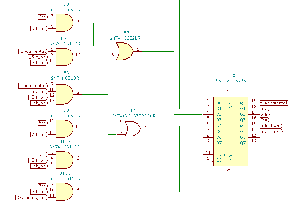
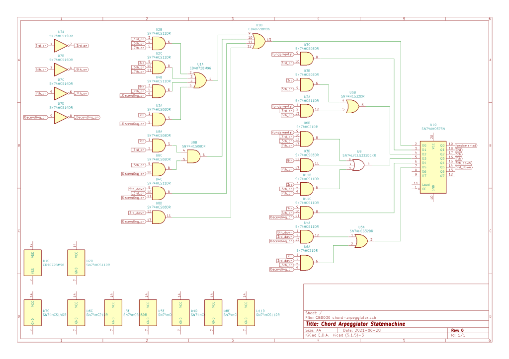
Previously in part 1 we diagramed a state machine to represent a chord arpeggio. In part 2 we determined what the sum of products would be for the state transition logic, and simulated the logic. Now it’s time for the next step which is to look at the physical implementation. I spent some time KiCAD and came up with this lovely schematic.
Ok so that’s 10 logic chips. We haven’t even looked at input conditioning, any manipulation of the clock that may need to be done, and actually generating an output control voltage from the various states. This is the point where I decide the module would be better implemented with a microcontroller, the scope expands out of control (because microcontrollers can do anything, why stop with 4-6 note sequences, why limit things to major and minor chords? What if I want to arpeggiate over a Cdim add 9 because I’m insane), and ultimately shelve the idea until a future date.
Last time I started designing a chord arpeggiator. We got as far as and articulating the specifications and then drawing a state machine to handle note transitions. Today we’ll try to minimize the gate count for transitioning between states and then simulate the logic using VHDL.
Logic Minimization
I decided to use Karnaugh Maps because I actually remember how to use them, and with only 8 variables the problem is still simple enough so that real logic minimization tools aren’t necessary yet. But ‘Aha!’ you say you have 10 variables 6 states and 4 inputs. Well since only one state can be active at a time the corresponding up and down states can be combined when working out the logic. To reduce typing I After working through the Karnaugh Map for each state I got this
States
Fundamental
Third
Fifth
Seventh
Fifth_down
Third_down
Inputs
Third_on
Fifth_on
Seventh_on
Decending_on
Logic
Fundamental = (not Third_on and not Fifth_on and not Seventh_on ) or (Third and not Fifth_on and not Seventh_on ) or ( Fifth and not Seventh_on and not Decending_on ) or ( Seventh and not Decending_on ) or ( Seventh and Decending_on and not Third_on and not Fifth_on ) or ( Fifth_down and not Third_on and Decending_on ) or ( Third_down and Decending_on )
Third = ( Fundamental and Third_on )
Fifth = ( Fundamental and not Third_on and Fifth_on ) or ( Third and Fifth_on )
Seventh = ( Fifth and Seventh_on ) or ( Third and not Fifth_on and Seventh_on ) or ( Fundamental and not Third_on and not Fifth_on and Seventh_on )
Fifth_down = ( Seventh and Fifth_on and Decending_on )
Third_down = ( Seventh and Third_on and not Fifth_on and Decending_on ) or ( Fifth_down and Third_on and Decending_on)
if I was actually good at digital design I’d be able to simplify that down to something ridiculous like 3 NAND and 2 XOR gates. But I’m not and that is a lot of logic which means there’s probably some errors in it and we should do a simulation.
Simulation
For simulating this type of glue logic I like to write a program for an FPGA and see how it runs. Of course I don’t have an actual FPGA or FPGA programming tool since they’re pretty spendy. So, I use the next best thing a web base FPGA simulator called EDA Playground because it’s free and easy to use. There are a variety of FPGA programming languages to choose from on EDA Playground. I picked VHDL because I remember how to use it the best of the available languages.
Link to EDA Playground arpeggiator simulation. While not my finest code it does show that the logic works. And EDA Playground provides a nice timing diagram for visualization.
Today’s Post is brought to you by my latest questionable module idea that probably only I am interested in. The idea is a four note chord arpeggiator. And not just four notes that would be boring I want to be able to toggle whether a note is played, toggle if the arpeggio is ascending only or will ascend and descend, and toggle some of the notes so the module can switch between major and minor chords and Major and Major 7 chords. Yes, I know just enough Baroque music theory to be dangerous. Back to the task at hand. And as always let’s try to do this without a microcontroller.
Specs
Up to 4 notes will be played
Notes 2-4 will be toggleable
Fundamental will be from CV input
2nd note is toggle able between major and minor 3rd
3rd note is a 5th above fundamental
4th note is toggleable between 7th and full octave
Output will be in 1 V/Octave
Changes to next note on clock pulse input
No micro
Design
If the module was going to transition between notes in a predictable order all the time we could use a shift register to handle the transitions. Since the transitions proposed are a little more complicated I decided to use a finite state machine to help design handle the transitions between notes.
What is a finite state machine? It is an abstract model of a system that can be in exactly one of a fixed number of states at a time. Such as a combination lock or a traffic light. Since we’ll only want to output one note of the chord at a time, and the clock input can indicate transition between notes/states, the state machine seems like a reasonable way to approach the problem.
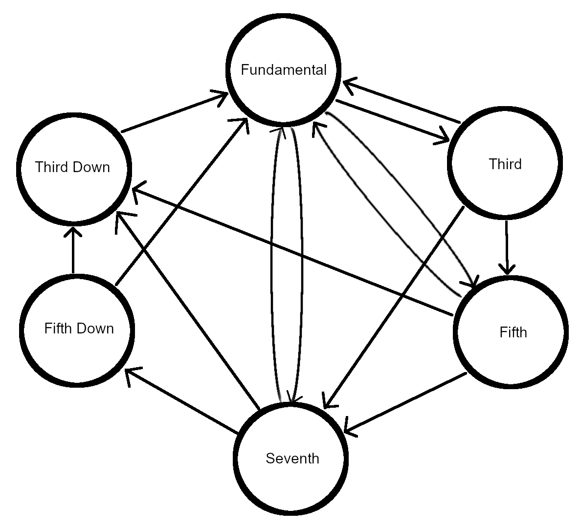
Next we’ll need to simplify thing a little bit Since it is unlikely that both the major and minor third would be played in the same sequence I went ahead and grouped those into the same state. Likewise the seventh and full octave states were grouped. I decided to give descending fifth and thirds their own states. The alternative would be to use a separate ‘current direction’ state, but this way seems lazier. We’ve got 6 states and I suspect it will be easy to find an 8 bit register/d-flop/latch block so no worries there. With the states defined all that remains is defining the transitions between the states. For that we’ll need to articulate the module inputs. I’ve come up with four inputs affecting the state machine
3rd Active
5th Active
7th Active
Descending Active
If the 3rd and 7th inputs are active and the 5th and Descending inputs are inactive that’ll produce note patterns of 1-3-7-1-3-7. If Descending is enabled the pattern will change to 1-3-7-3-1-3-7. This is going to get old fast so I’m just going to draw a graphical representation.
The circles represent the states the arrows represent possible transitions. If I were more ambitious I’d include some indication of the logic for each transition.
Join me next time when I start turning the graphical state machine into implementable logic.
After seeing how the ARP2600 implemented an ADSR. I’ve decided to pencil in the Decay and Sustain parts to my AR design.
Decay
Starting with the Decay stage. This will be similar to the Release stage. So we’ll just copy and paste the input mix and exponential converter. from that stage. Things diverge a bit with the current sink for decay because the output capacitor will be discharged to the sustain voltage instead of ground. So the fancy bi directional current source from the Release is getting replaced with a classic voltage controlled current sink design.
Decay Current sink
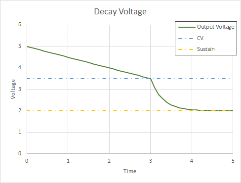
With this design if the control voltage is below the sustain voltage the MOSFET controlling current flow will be off. We can take advantage of this by using an enable to short the control voltage input to ground which will result in the current sink being off. It also means that the sustain voltage needs to be mixed with the decay control voltage in order to reliably discharge the output capacitor during the decay phase. The final note is that the size of the current sense resistor, R20, is going to have to be picked carefully. While the output voltage is higher than the control voltage the voltage change will be linear. Once the output voltage drops below the control voltage the op-amp will turn the current limiting FET, Q4, fully on and the remainder of the decay transition will be a regular RC discharge curve to the sustain voltage as seen below.
If we want to keep the linear voltage transitions from the Attack and Release stages then the current sense resistor needs to have a low value. However a low value resistor means a smaller control voltage range which means the system will be more susceptible to noise. The best solution here is probably to just try a couple values for the current sense resistor during prototyping and see how they sound.
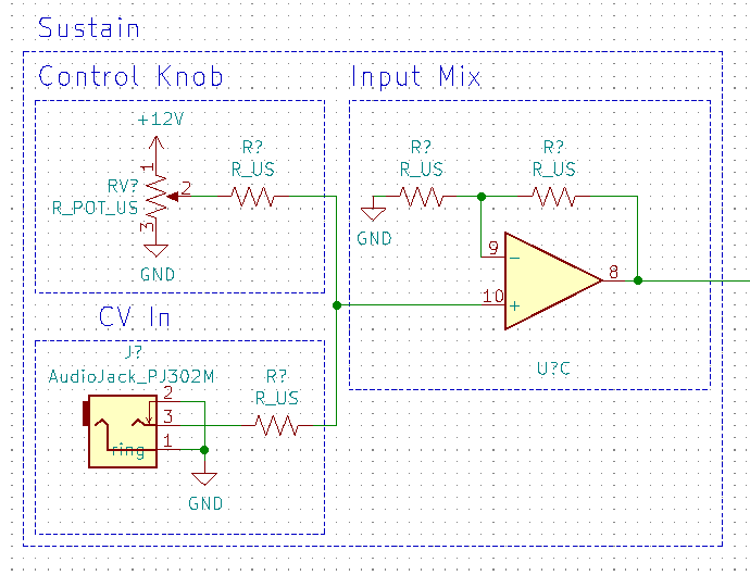
Sustain
Moving on to the sustain. The ARP2600 used a BJT, a capacitor and a potentiometer to set the sustain level. Since using CV is part of the design constraints it makes sense to use an op-amp to add the CV and control pot voltages. As the op-amp can perform the function of both the BJT and the capacitor in the original design we can drop those leaving us with.
Final Thoughts on the ADSR
This design uses fewer ICs than I was originally anticipating. I will probably try to prototype it at some point.
Previously I blocked in and picked some basic circuit designs for the Attack part of the AR module, and we learned some things looking at how the ARP2600 handled envelope generation. This time we’re going to expand the ‘control logic block’ to control when the capacitor is charging and discharging. Also I’ve picked out a few component values and calculated the range of control voltages and the range of charging currents and it looks like modifications will be needed. And lastly there’ll be a bit about the release block.
Controls
Last time we decided to ditching trying to time things and just use input and feedback control to enable charging the output capacitor. First the conditions for enabling the attack current source need to be described. The attack current source should be enabled if the Gate input signal is high and the output of the module is below the output set point. In circuit form that’s going to look something like this.
A comparator compares the current output with the setpoint. If the setpoint is higher than the output the comparator outputs a logic high value. If the gate is also high the AND gate outputs high and the Attack current source is enabled. A feedback resistor may need to be added to the comparator to prevent rapid toggling thus making the comparator a Schmitt Trigger. I also would like to note that this control set up will ‘top up’ the output capacitor if the gate is especially long and the capacitor begins to self discharge.
Math
This brings us to the part of the design where we need to pick some component values and transition times and start doing math to see if other component values are reasonable. Here are the initial choices.
Output Capacitor (C)
10 µF
Charge time min (tmin)
1 ms
Charge time max (tmax)
10 s
Output Voltage minimum (Vmin)
0 V
Output Voltage maximum (Vmax)
5 V
Now using the terminal equation for a capacitor
I = C dV/dt
and the input voltage output current relationship for the current source
Iout = 1/R * (Vcc – Vin)
The minimum and maximum charging currents and control voltages can be calculated.
Charge Time
Iout
Vin
1 ms
50 mA
2 V
10 ms
5 mA
11.9 V
1 s
50 µA
11.99 V
10 s
5 µA
11.999 V
Current Range
The output current range seems ok. 5 µA is on the small side, but we’ll have to actually build a prototype to see if it’s too small to work.
Voltage Range
The range for Vin however is immediately problematic for two reasons that require circuit adjustments.
First in order to have a long attack time Vin needs to be approximately the same as Vcc (on the order of 1 mV), and having inputs and outputs of an op amp at either of the power rails tends to cause unpredictable behavior. The ‘rail to rail’ op amps I usually use recommend operating 25 mV to 1 V from the rail for ideal performance. Additionally output current is related to the difference between Vcc and Vin. Vin is controlled and Vcc is 12 V, or is it? Vcc could be higher or lower depending on the power supply and the power input protection. The typical power input block I use for circuit protection and power filtering can drop the input voltage 10’s of mV. So referencing the control current to Vcc is going to cause unpredictable behavior.
So I’m swapping the current source for this one, which uses sources a current proportional to Vin, and has the added benefit of acting as a current sink, so an identical set up can be used as part of the release stage. A limiting factor here will be the maximum current output of the op amps and 50 mA is getting up there.
The second issue is that charge time and by extension input voltage covers 4 orders of magnitude. The table shows that input voltage difference between 1 s attack time and 10 s attack time is 9 mV while . So as is more of the input space for the module is devoted to short attack (and by extension release) times. This use of the input space is backwards to human perception that is it’s easier for humans to notice the difference between 1 s and 10 s than it is for us to notice the difference between 1 ms and 10 ms. So we want to convert a linear voltage input into an exponential voltage input to better match the control voltage to attack time to human perception. Fortunately there’s a pretty typical circuit for that.
Release block
At this point the release block is super easy. It’ll be identical to the Attack block with the following changes. The input voltage to the current source needs to be negative to make it a current sink. The control logic needs to be inverted. That is on when the gate signal is low and the output voltage is above 0 V.
A few days ago I came across the circuit diagram for the ADSR in the ARP 2600. After I got done being amazed at how the designers accomplished so much with just a handful of transistors, I learned a couple of things to bring back to my A(DS)R design. First a simplified version of the ARP 2600 ADSR schematic.
Simplified ARP 2600 ADSR
What’s been simplified? A substantial amount of circuitry has been replaced with ‘black (blue) boxes’ Their functionality is their outputs latch high (1) on event detection and reset low (0) some time after the gate signal falls to 0 (actual operation is more nuanced, but this description is sufficient for this discussion). Next, there are no actual logic gates in the original circuit; however, parts of the circuit function in a similar manner to logic gates. So these have been substituted. Finally, a number of ‘voltage controlled switches’ have been added. These are all transistors in the actual design. However, they are all different types of transistors (NJFET, PJFET, PNP) with different operating modes, and I wanted them all to have the same conceptual functionality for the sake of discussion. So they’ve all be replaced. The ‘voltage controlled switches function as follows a high control voltage closes the switch and a low control voltage opens the switch. (so they’re non latching relays).
Operation
Initial state
Prior to receiving a gate input the Release Switch is closed and the Memory Capacitor is drained to 0 V. The Sustain value is set via the npn transistor charging the Sustain Capacitor in the bottom right.
Gate Rising Edge
When the Gate signal goes high the release switch opens, and the rising edge control is set high. Since the other two detection blocks are still low the Attack Switch closes starting the note.
Gate on Attack ending
The Attack ends when the Memory Capacitor is charged to it’s maximum value somewhere between 8-10 V. The max value detection block is set high turning off the Attack Switch and turning on the Decay-Sustain Switch. Once the Decay-Sustain Switch is closed the Memory Capacitor drains through the Decay control until it reaches the same voltage as the Sustain Capacitor. Elegantly simple.
Gate Falling Edge
The last stage is the falling edge of the gate. The falling edge detection block is set high and the Decay-Sustain Switch is opened. Once the gate has transitioned to 0 V the Release Switch is closed, and the Memory Capacitor is drained through the Release Control. Once the Memory Capacitor is drained the cycle is read to begin again.
Take Aways
My first note is that a capacitor is used as the voltage value storage device, and there’s an op-amp buffer between the capacitor and the output. That’s exactly the configuration I chose. What a coincidence! Great minds think alike. Or there’s really only one device capable of storing analog voltages and that storage mechanism requires a high input impedance to low output impedance buffer to be useful to subsequent modules. Who knows?
The next note is that there is nothing resembling a timer anywhere in this. All transitions happen because of event detection and feedback. So I’m going to drop the timer from my design, and just use feedback. I might add it back in as part of the ‘trigger function’ but we’ll have to get further along in the design to see.
The last note is the simplicity of the Decay-Sustain portion of the circuit. I was originally thinking that I’d need two switches and a current source tuned to the the natural losses of the ‘memory’ capacitor for the Sustain. I was also anticipating needing a fair amount of components to control the transitions between the states. Now I’m thinking of doing a paper design for a voltage controlled Decay-Sustain in a similar vein to the this one to see how much complexity it would add.
The next module I’m designing is an envelope generator. Since, I’m doing this while I wait for boards and part for other modules, I’ve decided to do a better job documenting the early part of the deign; so, if this project gets shelved for a bit I can spend less time remembering where the design is at. Now on to the fun bits.
What is an Envelope Generator
In signals an envelope describes how the signal changes in time. Since I’m primarily working with synths, the signal is going to be sound. To make a synth envelope an envelope generator outputs a sequence of voltages that are typically used as control voltages for an amplifier or filter. For example an envelope (blue) is used to control the amplitude of a sine wave (pink) using a voltage controlled amplifier.
Envelope example
A Block Diagram
How do we create a sequence of voltages? To start with lets put together a block diagram for a four part envelope generator commonly referred to as an ADSR (attack, decay, sustain, release).
ADSR block diagram
I’ve expanded the A block to show likely sub-blocks the DSR blocks will contain similar sub-blocks. Working our way through the blocks. The inputs to the A stage, CV and control knob voltages, will be combined (probably added). The mixed control voltages will be fed to the driver block, where the control voltages will be interpreted into a signal to send to the memory block. The mixed control voltages will also be fed into a timer. When triggered the timer will close the switch between the driver and the memory block for a length of time determined by the control voltage. When the timer runs out the switch will open and the timer will signal that it is done to the control logic. On receiving a gate or trigger the control logic will trigger the timer connecting the stages driver to the modules memory block. When the control logic receives a ‘done’ signal from the timer in the current stage it will trigger the timer for the next stage. Articulating all of that makes me think about how easy it would be to do all of this with a micro controller. Which leads neatly into,
Constrains
Eurorack module -> size – power – jacks
Analog and glue logic components, no micro or purpose built ADSR chips
Needs to utilize CV
Only AR for first revision
Attack peaks at 5 V
If I was sane I would uses a custom made ADSR chip or a microcontroller to build this modules. However I’m a little deranged so for the paper design I’ll be sticking with analog and discrete logic components. If I discover that I’ll need an excessive number of logic chips I’ll probably redo the design with a micro controller before moving on to prototyping. Since I’m only mostly insane there will be some constraints to start decay and sustain stages will be dropped from the first version. And more than likely the peak attack value will be fixed at 5 V. Since the ADSR stages will have a lot of overlap I may revisit some of these choices after I do the component level design for the attack stage. And lastly this is nominally going to be a Eurorack module so I’ll be working inside that voltage and size restrictions as well. Also since this isn’t going to be part of a standalone synth it’ll use CV in addition to potentiometers to determine timing parameters.
Design Outline
Now the blocks can be roughed in. No math yet just picking out common design patterns to fill in the blocks, get an idea of component count that sort of thing.
Memory and Buffer
Were going to start with the easy sections first. For memory the classical analog memory element, a capacitor, seem like an appropriate starting point. and the buffer will be a high input impedance op-amp connected as a voltage follower.
Memory, Buffer, and Output stages
The astute among you will note that this is the ‘hold’ part of a sample and hold circuit, and I mentioned using a switch as part of the driver circuit which would be the ‘sample’ part. Whether this sample and hold will be implemented as discrete components or using a dedicated sample and hold IC will be determined later. Since the capacitor has four potential input ‘signals’ to sample from likely discrete components will be used.
Driver
As the memory component is a capacitor, a reasonable first choice for the driver is a current source (sink for D and R blocks). Right now the switch can be penciled in as an NMOSFET, but switching could be implemented by turning the current source off via the OpAmp inputs. Adding a current limiting resistor between the transistors will probably be a good idea as well.
Timer
The timer is going to need to generate a high voltage pulse to control the NMOSFET in the driver stage. A one shot is an option but a 555 timer comes with a handy control voltage (CV) input pin so that’ll be the starting point. When the ‘TR’ input is pulled low by the control logic the output, Q, will be driven high, and C will begin to charge. When the voltage on C exceeds the input control voltage the output will be driven low and the capacitor will be discharged through the DIS pin. So the values of R, C, and CV will determine on time. reset is penciled in to be always tied on however if the AR is retriggered before finishing ideally the entire process would start again from the beginning. So the reset pin may eventually be connected to the control logic.
Input and Input Mix
The final stage is the input mix. At least one op-amp will be needed to combine and buffer the inputs and adjust their range to match the input range of the driver and timer stages. A second op-amp is needed because the driver and timer stage need different control voltages to achieve the desired envelope shape. The op-amps as shown are connected in inverting configuration because it is anticipated that gains less than 1 will be required between the input and the output of the mix. however both driver and current stages as shown require positive input voltages so a third op-amp may be required. We’ll find out more once all of the math is done.
Everything so far
This is the design so far. I’ve added in a connection for output feedback to the input. Feedback control is almost always beneficial. Although until more of the design is fleshed out it’s not clear if the feedback will be more appropriate at the input or somewhere in the middle.
Next time we’ll do some math or think about the control logic or maybe both.