After seeing how the ARP2600 implemented an ADSR. I’ve decided to pencil in the Decay and Sustain parts to my AR design.
Decay
Starting with the Decay stage. This will be similar to the Release stage. So we’ll just copy and paste the input mix and exponential converter. from that stage. Things diverge a bit with the current sink for decay because the output capacitor will be discharged to the sustain voltage instead of ground. So the fancy bi directional current source from the Release is getting replaced with a classic voltage controlled current sink design.

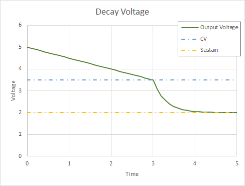
With this design if the control voltage is below the sustain voltage the MOSFET controlling current flow will be off. We can take advantage of this by using an enable to short the control voltage input to ground which will result in the current sink being off. It also means that the sustain voltage needs to be mixed with the decay control voltage in order to reliably discharge the output capacitor during the decay phase. The final note is that the size of the current sense resistor, R20, is going to have to be picked carefully. While the output voltage is higher than the control voltage the voltage change will be linear. Once the output voltage drops below the control voltage the op-amp will turn the current limiting FET, Q4, fully on and the remainder of the decay transition will be a regular RC discharge curve to the sustain voltage as seen below.
If we want to keep the linear voltage transitions from the Attack and Release stages then the current sense resistor needs to have a low value. However a low value resistor means a smaller control voltage range which means the system will be more susceptible to noise. The best solution here is probably to just try a couple values for the current sense resistor during prototyping and see how they sound.
Sustain
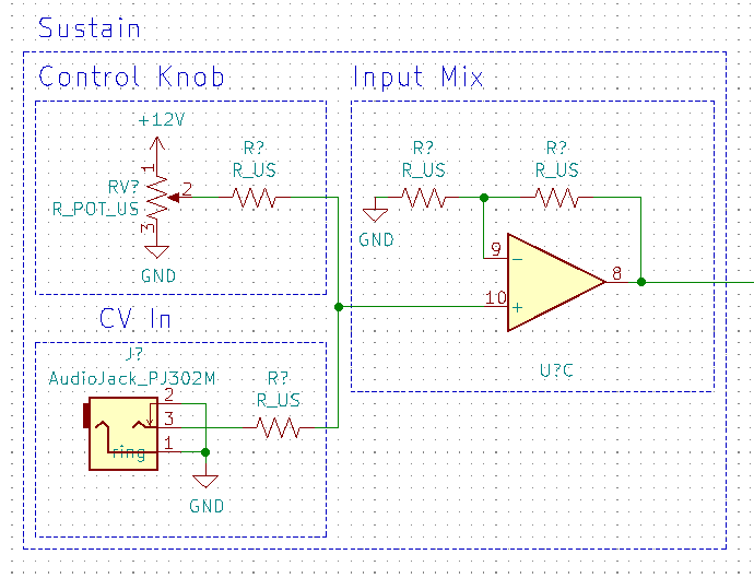
Moving on to the sustain. The ARP2600 used a BJT, a capacitor and a potentiometer to set the sustain level. Since using CV is part of the design constraints it makes sense to use an op-amp to add the CV and control pot voltages. As the op-amp can perform the function of both the BJT and the capacitor in the original design we can drop those leaving us with.
Final Thoughts on the ADSR
This design uses fewer ICs than I was originally anticipating. I will probably try to prototype it at some point.
